


 분야
분야2. Photolithography
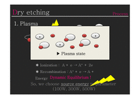
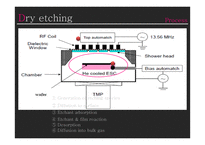
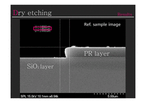
3. Etching
4. Metal deposition
5. Silicidation
6. QnA
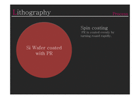
Si Wafer coated with PR
Spin coating
PR is coated evenly by turning round rapidly.
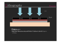
Exposure
Align the Mask exactly and emit UV.(fixed 10sec)
Observation
See the completed sample through SEM
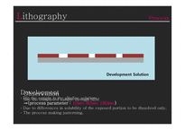
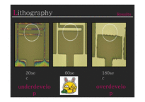
Development
∙ Dip the sample in the alkaline solution.
→(process parameter : 10sec 60sec 180sec)
∙ Due to differences in solubility of the exposed portion to be dissolved only.
∙ The process making patterning.


