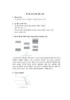
어떻게?
① Metal을 이용
☞ Contact Resistance ↓, but Transmittance ↓
② Graphene을 이용
☞ Transmittance ↑, but Contact Resistance ↑
③ Metal/Graphene layer를 이용
☞ Transmittance ↑, Contact Resistance ↓
④ Patterned metal + Graphene을 이용 !! ↕:Good
☞ Transmittance ↑↑, Contact Resistance ↓↓ ↕: Bad
contact to p-GaN with low resistance is essential for
achieving GaN-based LED with better efficiency.
Desired : Low contact resistance to p-GaN and High transmittance.
① Metal layer
☞ Low Contact Resistance, but Low transmittance
② Graphene layer☞ Excellent Transmittance, but High contact resistance
③ Metal/Graphene layer to p-GaN☞ Improved contact resi
band of the two semiconductors determines a charge transfer,
creating a triangular potential.
3. Polarization
- AlGaN/GaN HEMTs transistor don’t need doping to obtain a high electron density.
4. Contacts
- Source / Drain : Ohmic contact, Carrier could move free Metal ↔ Semiconductor.
- Gate : Schottky contact, controlled transistor to turn on / off.
5. Summary
9. n-type Semiconductor에서 온도에 따른 Carrier 농도 변화
매우 낮은 온도에서는 intrinsic EHP가 거의 존재하지 않는다. 온도가 증가함에 따라 도너의 전자들이 Conduct band로 옮겨지고 약 100K에서 모든 도너 원자가 이온화되는 과정이 발생한다. 이후 ni가 Nd와 비등해 질 때까지(intrinsic carrier 농도가 도너 농도와
5.2 Drug Delivery System
5.2.1 Advantage of Nano-drug delivery system
By diagnosis, and for treatment, we need enhanced drug delivery system. Drug delivery system of these days is just eat and let it flow through the body. It is not good at efficiency. Because the digestive system sometimes digest and remove the drug before it reaches to the target.
For enhancing the efficiency of drug