ML2 means the maskless lithography. It is necessary to refinement process. Described above, "double / mutiful patterning" in additional cost savings as an alternative to be appropriate. Nano devices with decreasing the size of the unilateral use light to produce a mask for the lithography process takes time and cost. Small production of nano scale patterning process is suitable, and the suitable
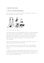
이미지 처리 시스템(그림 1.1)은 장면을 비추기 위한 광원, 센서 시스템(보통 CCD 카메라) 그리고 센서 시스템과 컴퓨터 사이의 인터페이스로 구성된다.
그림 1.1 이미지 처리 시스템의 구성요소들
다른 것들 중에서 인터페이스는 아날로그 정보를 컴퓨터가 이해할 수 있는 디지털 데이터로 변환한다.
65 535게의 색깔을 지지하는 시스템이면 각 색깔이 저장하고 회복할 수 있는 서로 다른 값을 가진다. 디지털 카메라에 들어가는 CCD는 예전의 기술과 비교하면 해상도를 더 많이 향상하게 된다. 더군다나, 어떤 디지털 카메라에는 100만게 넘은 픽슬을 생성하고 있지만 100달러정도만 팔게 된다. 그런 카메
(4) Double patterning
The double patterning is divided into four parts, leading with wafer requirements and then two sets of lithographic requirements (Generic Pitch Splitting - Double Patterning Requirements Driven by MPU metal Half-Pitch and Generic Spacer Patterning Requirements - Driven by Flash). The lithography requirements are different for each process; the requirements for pitch splitti
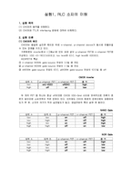
1. 실험 목적
(1) CMOS의 동작을 이해한다.
(2) CMOS와 TTL의 interfacing 방법에 대하여 이해한다.
2. 실험 이론
(1) CMOS의 원리
CMOS는 동일한 실리콘 웨이퍼 위에 n-channel, p-channel device가 동시에 만들어질 수 있는 장점을 가지고 있다.
기본회로는 inverter로서 <그림a>에 있는 바와 같이 p-channel FET와 n-channel F