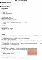
etching
SiO2
N-type
Si
N-type
SiO2
⦁SiO2 that does not have PR is removed by wet etching and also remaining PR is removed by acetone.
Source Drain Opening
○ SiO2 Deposition ( 100nm ) ○ PR(positive) Coating
SiO2
SiO2
N-type
Si
N-type
SiO2
⇒
PR
SiO2
SiO2
N-type
Si
N-type
SiO2
1. 서 론
1.1 LED를 왜 쓰는가?
LED(Light Emitting Diode)는 전기에너지를 빛에너지로 변환시켜주는 발광반도체로서, 1995년에 고휘도 녹색 LED가 개발됨에 따라 빛의 삼원색인 적색, 청색, 녹색 LED가 이용가능하게 되었으며, 1996년에는 청색 LED에 YAG:Ce 계열의 형광물질을 도포한 백색 LED가 개발되면서 차세대
1. 용접의 개념
금속과 금속을 충분히 접근시키면 이들 사이에는 뉴튼의 만유인력에 따라 금속 원자간에 인력이 작용하여 서로 결합하게 된다. 이 결합을 이루려면 원자들을 10nm정도 접근시켜야 하는데 이와 같은 일은 평상시에는 일어나지 않는다. 그 이유는 보통조건에서는 금속표면에 산화막이 존
- 가장 보편화된 나노기술현재 인간이 가지고 있는 보편화된 기술 중 가장 미세한 구조물을 만들어내는 방법이 있다면 그것은 포토리소그래피일 것이다.포토리소그래피는 실제 전자집적회로> 제작에 사용되는 기술로써 그 원리는 다음과 같다.크롬층과 유리기판의 맨 위에 놓인 감광고분자 막 위에 레
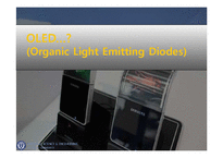
First, Substrate is consists of a plastic or glass, a portion of the OLED is supportive.Anode is a role that make electron holes when current flows by removing electron. And the upper Conducting Layer is the place that Electron Holes is being created.Emissive Layer is the place accepting an electron from Cathode and produce light.
Emissive layer and conducting layer are called organic layer beca