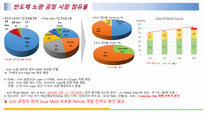
1. 반도체 노광 공정 시장 점유율
2. EUV용 Pellicle 시장 규모 및 개발 현황
3. EUV용 Mask 기술 현황_1(Mask Writing 장비)
4. EUV용 Mask 검사 기술 현황 및 시장 규모_1
5. EUV용 Mask 검사 기술 현황 및 시장 규모_2
6. EUV용 계측 기술 현황 및 시장 규모
대학 물리학과 현대 광학 이라는 수업에서 제출했던
광학과 관련된 최근의 기술에 대한 레포트입니다
EUV Lithography와 관련 광학 기술에 대한 기사 및 발췌 형식으로
광학 기술과 관련 기술의 응용 원리 및 수식 등이 설명되어 있습니다.
많은 도움이 되시길 바랍니다.
3. Requirements of EUV resist
EUV is highly absorbed by all materials, even EUV optical components inside the lithography tool are susceptible to damage, mainly manifest as observable ablation. Such damage that is associated with the high-energy process of generating EUV radiation is a new concern specific to EUV lithography .
EUVL's shorter wavelength also increases flare, resulting in less
ML2 means the maskless lithography. It is necessary to refinement process. Described above, "double / mutiful patterning" in additional cost savings as an alternative to be appropriate. Nano devices with decreasing the size of the unilateral use light to produce a mask for the lithography process takes time and cost. Small production of nano scale patterning process is suitable, and the suitable
(4) Double patterning
The double patterning is divided into four parts, leading with wafer requirements and then two sets of lithographic requirements (Generic Pitch Splitting - Double Patterning Requirements Driven by MPU metal Half-Pitch and Generic Spacer Patterning Requirements - Driven by Flash). The lithography requirements are different for each process; the requirements for pitch splitti