The threshold voltage of a MOSFET is usually defined as the gate voltage where an inversion layer forms at the interface between the insulating layer (oxide) and the substrate (body) of the transistor. The purpose of the inversion layer's forming is to allow the flow of electrons through the gate-source junction. The voltage of oxide is given by
V_OX= 1/C_OX 2√(qN_A ε_Si V_0 )
SiO_2 V_O
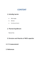
2. Thermal Equilibrium
Fermi level for the first time (Figure 3(c)) of the dash-dot line) is drawn.
Semiconductor conduction band and valence band of the neutral zone draw. To display the semiconductor doping level of Fermi level for the proper placement of the band (as shown in Figure 3-a in the neutral zone - energy band diagram, the same must be present.
In depletion layer
2.3 C-V graph
The measured MOS capacitance (called gate capacitance) varies with the applied gate voltage.
① Measurement of C-V characteristics
-Apply any DC bias, and superimpose a small (15 mV) ac signal
-Generally measured at 1 MHz (high frequency) or at variable frequencies between 1KHz to 1 MHz
-The dc bias VG is slowly varied to get quasi-continuous C-V characteristics
② C-V chara
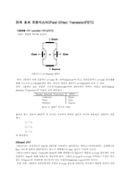
그림13-2는 정상적으로 bias된 JFET를 나타낸다. BJT에서는 베이스-에미터간에는 순방향으로 bias 되는데 반하여 JFET에서는 반드시 역방향으로 bias 된다는 사실이 다르다.
그림13-2에서 Gate는 Source와 Drain에 대해 역방향으로 bias되기 때문에 n-type 반도체의 전하운반자는 Gate에 대해 먼쪽으로 이동하게 된다. 그
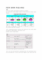
N채널 p채널이라는 표시는 drain과 source가 연결된 물질에 따라 표시 된다.
간단한 n채널 JFET가 [그림4]에 나타나 있다. 여기서 drain과source는 n 채널에 연결되 있고
gate는 p채널에 연결되어 있다. N 채널 반도체에 p 채널을 도핑하여 P-N 접합을 만드는 것이다.
이때 drain에 (+), source에 (-)를 걸어 주면 전류는