The threshold voltage of a MOSFET is usually defined as the gate voltage where an inversion layer forms at the interface between the insulating layer (oxide) and the substrate (body) of the transistor. The purpose of the inversion layer's forming is to allow the flow of electrons through the gate-source junction. The voltage of oxide is given by
V_OX= 1/C_OX 2√(qN_A ε_Si V_0 )
SiO_2 V_O
Ⅰ. 개요
반도체 물질에서 전기를 나르는 물질에는 전자와 홀(Hole: 구멍, 즉 전자가 빠진 자리라는 뜻) 이라는 것도 있다. 전자는 마이너스(Negative)전기를 가지고 있다. 전자가 많은 반도체를 N타입 반도체라 하고 홀이 많은 반도체를 P타입 반도체라고 한다. N타입이나 P타입 반도체는 반도체에 첨가하
we use Sputter?
- Good for high Melting point Material
- Thickness uniformity
- Positive adhesion
- But, law growth rate and step coverage
Patterning : Photo Lithography
(Clear than Shadow Mask)
Why Al is used for electrode?
(Especially Gate)
- Law melting point
- Work function
- High-K, Good mobility
- Elimination of carrier mobility degradation
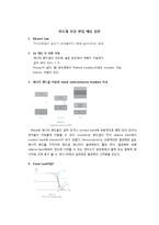
9. n-type Semiconductor에서 온도에 따른 Carrier 농도 변화
매우 낮은 온도에서는 intrinsic EHP가 거의 존재하지 않는다. 온도가 증가함에 따라 도너의 전자들이 Conduct band로 옮겨지고 약 100K에서 모든 도너 원자가 이온화되는 과정이 발생한다. 이후 ni가 Nd와 비등해 질 때까지(intrinsic carrier 농도가 도너 농도와
유리기판 (glass)
Glass를 TFT line 투입 전 Cleaning
이용하여 Glass표면에 묻어 있는
불순물을 제거
Gate 전극 생성 (Gate electrode)
Sputtering에 의하여 Gate 금속막 증착
절연막 및 반도체막 생성
(Insulator & a-si)
Photography에 의하여 생성
Date 전극 생성 (Date electrode)
Etching으로 Glass위에 증착된 금속막의