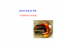
Layers>
- SiO2의 부도체 성질로 부터 집적회로내 금속층
사이의 효과적인 절연체로 사용가능
- 오염물질의 확산을 최소화
자연 산화물 – 오염물질이 대부분. (기억저장 공간이나 막 안정화용 사용)
게이트 산화물 – 트랜지스터의 게이트와 소스/드레인의 유전체로 사용
자계
The threshold voltage of a MOSFET is usually defined as the gate voltage where an inversion layer forms at the interface between the insulating layer (oxide) and the substrate (body) of the transistor. The purpose of the inversion layer's forming is to allow the flow of electrons through the gate-source junction. The voltage of oxide is given by
V_OX= 1/C_OX 2√(qN_A ε_Si V_0 )
SiO_2 V_O
layer, it causes entire curve of graph to shift to the [Figure 12] C-V graph shift by direction of bias
side. These charges are generated by ions came in the process of deposition of oxide layer. When the charges exist in between the substrate and interface, the value of Vfb and C-V curve will shift by amount of the charge divided by Cox of Ci. The amount of shifting decreases as the position of
Layer의 제1층), 또는 물리계층 인터페이스, DTE/DCE 접속방법, 그냥 인터페이스 등으로 부르는 것이 더 현실적일 것이다.
세계 시장에는 여러 제조업자들이 생산한 수많은 종류의 DTE나 DCE가 나와 있다. 그런데 만일 이들 DTE나 DCE간을 상호 연결하기 위한 접속규격이 정의되어 있지 않다면 이들을 접속하
Layer의 물리계층을 의미하며, 인터페이스 또는 DTE/DCE 접속규격, RS-232C 접속규격 등 여러 가지 의미로도 불리운다.
DTE/DCE 접속규격은 다음 4가지 중요한 특성을 갖고 있다.
� 기계적 특성(Mechanical 특성) : ISO 2110 규격
� 전기적 특성 (Electrical 특성) : ITU-T V.28 규격
� 기능적 특성 (Funct