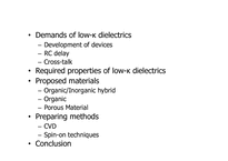
1 GPa
Elastic modulus Nanoindentation > 6 GPa
Adhesion Tape pull, modified-edge lift-off Delamination-free
Disavantages
Weakens mechanical properties
Lower thermal conductivity
Narrow pore distribution to ensure dielectric constant is homogeneous and isotropic
Pores need to be closed cells to prevent crack propagation and moisture absorption
Need to add silica to seal surface pores
첫째 저는 반도체 및LED 공정에 대한 이해도가 높습니다.
② Cleaning/Dry Etching 단위 공정 Engineer로써 단위 공정 Set up
및 공정불량 개선(SEM/FIB이용) , CI , 신규공법 적용 및 Max. Capa.활동
둘째 저는 반도체/LED 신규 장비에 대한 공정 Set up 경험이 많습니다.
① 반도체 200/300mm Cleaning 장비 (WET/Single)
② LED
First , I have high understanding about semiconductor and LED process.
Second, I have a lot of experience that set up the new machine .
① In Semiconductor Line , 200/300mm Single Spin Cleaning Machine.
Third , I have a lot of experience that apply new method to Unit Process and development of Cleaning/Dry Etching Process
Forth, recently I finished 3D Products Modeling in Korea machiner
PERSONAL DATA
Name: Hong Gil Dong
Address: 3floor giheung-gu giheung -dong, Gyeonggi-do, Korea ,
Cell Phone: xxx-xxxx-xxxx
E-mail: sss@naver.com
Date of Birth: Jan 8,1999
Sex: Male
* EDUCATION:
xxx University in Kyonggi (1999.03-2005.02)
Specialized in Electoronic Engineering
Graduate Index: x.xx/4.5
TOEIC score: 735 (2004.12), Toeic speaking score: 110 (