The lens is used to focus the sectioned UV light down to a smaller area on the chip. The smallest feature size capable of being written on the wafer is a function of the numerical aperture of the lens as well as the wavelength of the light.
uses a patterned elastomer(e.g. PDMS(Poly DiMethyl Siloxane)) as the stamp, mold, or mask to generate micro-patterns and microstructures
C
What is soft-lithography?
So, an alternative and non-photolithographic method that we call soft lithography was developed. Because this method uses a patterned elastomer(e.g. PDMS(Poly DiMethyl Siloxane)) as the stamp, mold, or mask to generate micro-patterns and microstructures, it was titled as 'soft' lithography. As compared with photo-lithography, soft lithography has many kinds of strength.
- 유기 EL (OLED; Organic Light Emitting Device or Diode) -
1. 유기 EL이란?
유기 EL(OLED; Organic Light Emitting Device or Diode)은 유기물(저분자 또는, 고분자) 박막에 음극과 양극을 통하여 주입된 전자(electron)와 정공(hole)이 재결합(recombination)하여 여기 전자(exciton)를 형성하고, 형성된 여기 전자로부터의 에너지에 의해 특
1. 외부 양자 효율을 높일 수 있는 방법
1) 수직구조 발광다이오드를 사용한 양자 효율 증가 방법
2) 다공성 알루미나를 사용한 양자 효율 증가 방법
-알루미나를 이용한 OLED의 전기적 광학적 특성을 조사한 결과, 전기적 특성은 소자 내부의 구조가 같으므로 큰 차이가 없다는 것을 알았다. 그러
Understand
Principles of micro-scale patterning process
Experiment
Display devices and MEMS, Developing micro-channel
MEMS
(Micro-Electro-Mechanical Systems)
Technology of very small mechanical devices
What for, MEMS ?
Chemistry, Biology, Medical Science, Mechanics, Electronics
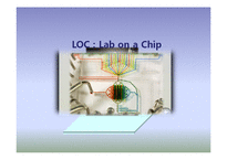
Why, Lab-On-a-Chip ?
Several Lab functions on a single chip
very Small size
Cheap – Mass