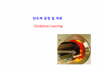
4. Dopant Barrier <불순물 장벽>
- 산화층이 실리콘 표면에서 성장하면 불순물 물질이 wafer로 들어가는 곳에 창을 생성시키기
위해서 Mask 개방으로 SiO2를 식각, 이때 산화물은 dopant의 확산으로부터
silicon의 표면을 보호.
- 선택적인 dopant의 도핑가능
5. 금속층 사이의 유전체
Like a finger in the macro world so feels a tiny tip on a lever in the nano world a surface Forces are in Pico Newton range the same like intermolecular binding forces
1-1. AFM tip
- actually feels the sample surface.
- siliconnitride
exhibit excellent flexibility, Contact AFM mode
- silicon crystal
high frequency oscillating(100kHz), more stiffer than siliconnitride, non co
캔틸레버의 탐침은 시료표면에 적용되는 힘이나 AFM의 lateral resolution을 결정.
Silicon , siliconnitride로 만듦
길이 100-200㎛, 넓이 40㎛, 두께 0.3-2㎛
표면에 수직하게 야기되는 반발력
반발력은 1~10 nN
작은 힘에도 매우 민감하게 반응하여 0.01 nm 정도로 미세하게 움직이는 것까지 측정
미세한 표면형상
silicon is on the gas SiH2Cl2, of which it is at relatively low temperatures separates.
⇒ With the support of the plasma excitation are the low process temperatures at 300℃ is possible.
⇒ The deposition of SiO2 and siliconnitride Si3N4 at low conformity.
⇒ High growth speed up to 500 nm/min is possible.
∙ Deposit at low temperature because of plasma.
∙ High vacuum a
소성, 유약칠, 채식 등의 복잡한 과정을 거치지만 원하는 모양, 색을 성형하기 유리하다.
Zirconia(ZrO2
1500℃이상에서 소결하여 얻으며 다른 원소를 첨가하여 다양한 색을 얻을 수 있다.
SiliconNitride(Si3N4)
소결에 의해 형성되기 어려우므로 1400℃의 높은 온도에서 촉진제를 첨가해야한다.