(4) Double patterning
The double patterning is divided into four parts, leading with wafer requirements and then two sets of lithographic requirements (Generic Pitch Splitting - Double Patterning Requirements Driven by MPU metal Half-Pitch and Generic Spacer Patterning Requirements - Driven by Flash). The lithography requirements are different for each process; the requirements for pitch splitti
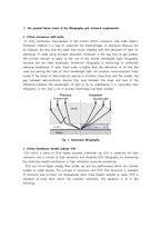
ML2 means the maskless lithography. It is necessary to refinement process. Described above, "double / mutiful patterning" in additional cost savings as an alternative to be appropriate. Nano devices with decreasing the size of the unilateral use light to produce a mask for the lithography process takes time and cost. Small production of nano scale patterning process is suitable, and the suitable
1장. Introduction
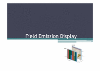
FED는 평판표시소자의 하나로 양극과 사이의 강한 전계에 의해 각 픽셀의 전자총으로부터 방출된 전자가 형광체에 충돌하여 형광체에서 빛을 발하는 현상을 이용한 표시소자이다. 이와 같은 FED는 넓은 시야각, 우수한 해상도, 낮은 구동 전압, 온도에 대한 안정성 등 기존의 CRT에 비해
1.1 TFT-LCD의 정의 및 특징
TFT(Thin Film Transistor)는 박막트랜지스터는 3개의 단자에 의해 구동되어 지며 전기적인 관점에서 볼 때 전계효과 트랜지스터(FET)의 종류이다. 그리고 금속-산화물-반도체 전계효과 트랜지스터(MOSFET)와 유사한 특성을 갖는다. TFT에 사용되는 재료로는 비정질실리콘, 다결정실리