도핑 준위
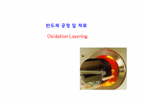
Model : Deal & Grove의 선형-포물선 모델<300 Å - 20,000 Å> 의 성장
150Å까지는 선형적인 산화층의 성장
X = (B/A)t
X : 성장 산화물의 Thickness
B/A : 선형 비례 상수
T : 성장시간
150Å이후는 포물선식 산화층의 성장
X = (Bt)1/2
X = 산화물의 성장 Thickness
B : 포물선 속도 상수
T : 성장시간
Making the Wafer
The process
-A seed crystal is suspended in a molten bath of silicon
-It is slowly pulled up and grows into an ingot of silicon
-The ingot is removed and ground down to diameter
-The end is cut off, then thin silicon wafers are sawn off (sliced) and polished
Epitaxy
The growth of an ultra-pure layer of crystalline silicon
Approx 3% of wafer thickness
Contaminant-free
layer, it causes entire curve of graph to shift to the [Figure 12] C-V graph shift by direction of bias
side. These charges are generated by ions came in the process of deposition of oxide layer. When the charges exist in between the substrate and interface, the value of Vfb and C-V curve will shift by amount of the charge divided by Cox of Ci. The amount of shifting decreases as the position of
Ⅰ. 서론
CAD란 연필, 붓, 물감 등의 도구들을 이용해 지면에 여러 가지 형상을 표현한 그림이나 설계도면처럼 모니터라는 종이 위에 마우스나 키보드, 스캐너, 디지타이저 등의 입력 장치를 이용하여 어떤 형상을 표현하는 것이다. 그렇다면 붓과 종이로 그림을 그리고 설계를 하는 것과 컴퓨터를 이
The threshold voltage of a MOSFET is usually defined as the gate voltage where an inversion layer forms at the interface between the insulating layer (oxide) and the substrate (body) of the transistor. The purpose of the inversion layer's forming is to allow the flow of electrons through the gate-source junction. The voltage of oxide is given by
V_OX= 1/C_OX 2√(qN_A ε_Si V_0 )
SiO_2 V_O