9. n-type Semiconductor에서 온도에 따른 Carrier 농도 변화
매우 낮은 온도에서는 intrinsic EHP가 거의 존재하지 않는다. 온도가 증가함에 따라 도너의 전자들이 Conduct band로 옮겨지고 약 100K에서 모든 도너 원자가 이온화되는 과정이 발생한다. 이후 ni가 Nd와 비등해 질 때까지(intrinsic carrier 농도가 도너 농도와
ohmic contact to p-GaN with low resistance is essential for
achieving GaN-based LED with better efficiency.
Desired : Low contact resistance to p-GaN and High transmittance.
① Metal layer
☞ Low Contact Resistance, but Low transmittance
② Graphene layer☞ Excellent Transmittance, but High contact resistance
③ Metal/Graphene layer to p-GaN☞ Improved contac
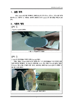
ohmic contact을 형성하는 contact layer로 사용되어 왔다. 하지만 NiCr은 훌륭한 안정성과 TCR 특성을 갖고 있음에도 불구하고, NiCr은 습기에 대한 부식을 느끼기 쉽다. Gold층과 Si층은 접착성이 떨어지지만 gold층은 얇은(약 50nm) NiCr층과의 접착성이 상대적으로 우수하다. 반도체공정 중에는 다양한 anneal과정이 있
band of the two semiconductors determines a charge transfer,
creating a triangular potential.
3. Polarization
- AlGaN/GaN HEMTs transistor don’t need doping to obtain a high electron density.
4. Contacts
- Source / Drain : Ohmic contact, Carrier could move free Metal ↔ Semiconductor.
- Gate : Schottky contact, controlled transistor to turn on / off.
5. Summary