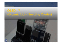
First, Substrate is consists of a plastic or glass, a portion of the OLED is supportive.Anode is a role that make electron holes when current flows by removing electron. And the upper Conducting Layer is the place that Electron Holes is being created.Emissive Layer is the place accepting an electron from Cathode and produce light.
Emissive layer and conducting layer are called organic layer beca
sub-threshold 영역에 10배의
drain current를 변하게 하기 위해 필요한 gate voltage의
증가량이다. 이 swing값은 sub-threshold영역에서 Vgs의
값에 따라 얼마나 급격히 drain current가 변하는 지에 대
지표인데, 스윙 값이 작을수록 작은 Vg의 변화에도 Id가 급
격히 변하는 것을 의미하므로 transistor가 off 상태일 때
lea
: two metal depositions followed by an oxidation and a further metal deposition from a different angle form an overlap of two stripes
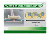
Why GaAs quantum dot ?
Proper quantum dot size enough to be placed between source and drain by using templates-based technique
2) Band gap of GaAs (1.42eV~1.52eV) higher than basic thermal energy (0.0259eV)
3) GaAs quantum dot has Coulomb blockade
oxide)막이 형성되어 있다. 전극 위에는 액정 방향자의 방향이 결정될 수 있도록 수백ANGSTROM 정도의 배향막을 도포하여 상판과 하판에서의 배향 방향이 서로 수직이 되도록 러빙처리한다. 그러면 전기장이 인가되지 않은 상태(비활성 상태)에서 액정 방향자는 한 기판에서 다른 기판으로 연속적으로 90 DEG
Sub-15nm Resolution by Zhiwei Li, Yanni Gu, Lei Wang, Haixiong Ge, Wei Wu, Qiangfei Xia, Changsheng Yuan, Yanfeng Chen, Bo Cui, and R. Stanley Williams. NANO LETTERS 2009 Vol.9, No.6 2306~2310"
Article : To achieve high resolution patterning
Soft lithography commonly uses PDMS to stamp. It enables a conformal contact with substrates or the master mold over a large area without applying exter