Phosphor (Energy Converter)
Inorganic phosphor materials
“Classical” inorganic phosphors usually consist of a host lattice with activator ions doped into it in small concentrations, typically a few mole percent or less.
Host lattice & Activator ion
1st type : weak interaction (Ln3+)
2nd type: strong interaction ( Mn2+, Eu2+, Ce3+, Pb2+,Sb3+, Ce3+, MoO42-, NbO43-)
Activator (+ Sensit
1. Nanorods
of the reported procedures for rod formation, seedmediated growth has been by far the most efficient and popular approach. The role played by the seed particle is also critical. Furthermore, the presence of small amounts or silver nitrate during the synthesis has a dramatic effect on the final shape and crystalline structure if the particles. Citrate-capped gold nanoparticle, prepare
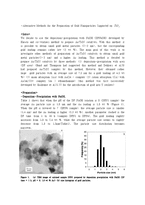
nanostructure with lengths of several decade microns. The high-magnification images of single ZnO nanostructure in Fig. 1(d) and (e) reveal that they are composed of central axial nanowires surrounded by radially oriented nanorods with 6-fold structural symmetry. Fig. 1(f) shows the side-wall image of hierarchical ZnO nanostructure with widths of 70–-120 nm and average length of around 600
The ZnO and ZnMgO nanostructures were grown on silicon substrates at different temperatures, using gold metal as a catalyst in the presence of argon as a carrier gas in a conventional tube furnace.
The effects of the substrate temperatures, gold catalyst, and source material preparation on the morphological and optical properties of the nanostructures were investigated.
Si substrates were c
∙ ZnO is an good candidate for fabrication of optoelectronic
and electronic device.
∙ 1D ZnO nanostructures have many properties.
∙ It is that a simple two-step thermal evaporation process
to synthesize the hierarchical pure ZnO nanostructures of 6-fold structural symmetry without any metal catalyst.
∙ Pure zinc powder(99.99%)
nanostructures, nanostructured materials, nanoimprint, nanobiotechnology, nanophysics, nanochemistry, radical nanotechnology, nanosciences, nanooptics, nanoelectronics, nanorobotics, nanosoldiers, nanomedecine, nanoeconomy, nanobusiness, nanolowyer, nanoethics’. ‘to be nano or not to be nano?’, Christian Joachim, nature materials, vol 4, February 2005
[그림 1-1] 은 나노기술의
1.1 Soft lithography
Microstructure나 nanostructure을 만들기 위한 printing, molding의 과정을 포함하는 technique으로, 일반적으로 printing, molding, transfer의 3단계 과정을 거친다.
1.1.1 Printing
Master를 만드는 과정이다. Photolithography, e-beam, micro-machining, photoresist 등 다양한 방법을 통해 원하는 모양을 가지는 master를 제작할
properties
investigating transition metal oxides
specific morphologies
nanostructured materials
→ the charge storage from faradaic processes occurring at the surface of the material
→ the pseudo-capacitive effect, becomes increasingly important
mesostructured materials
→ enhanced oxidation and reduction kinetics
→ the relatively short diffusion path length for ions and electrons
nanostructure을 구현하면 capillary force에 의해 필터는 초발수성과 초친유성을 가지게 된다. 물은 필터를 통과할 수 없지만 기름은 통과할 수 있게 되는 것이다. [1]
또한 ZnO는 광촉매의 성질을 가지고 있기 때문에 UV를 조사하면 필터는 초발수성에서 초친수성으로 성질이 변하게 된다. 이러한 특성 변화를
Direct wide band gap : 3.37eV
Large excitation binding energy : 60 meV
Piezoelectronic material
One dimensional ZnO in oxide nanostructures
Safety is best
Toxicity is less than other materials
ZnO carry out a role of UV rays by itself
Aligned ZnO nanowires are grown vertically
on silicon substrates by carbothermal route
Aligned ZnO nanowires are grown
wit