for high Melting point Material
Positive adhesion
But, EBE is possible x-ray damage
- High Pressure for Plasma
- Power for Frequency
- Gas concentration
- Deposition : 100nm
Why we use Sputter?
- Good for high Melting point Material
- Thickness uniformity
- Positive adhesion
- But, law growth rate and step coverage
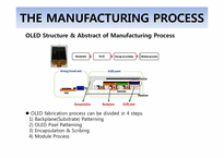
Patterning : Photo Lithography
electron composed of metal
Anode : injecting hole composed of transparent ITO
Emissive polymer : recombination between hole and electron
Conducting Polymer : transporting holes
For many reasons; Less weight, flexible, fast response, lower power consumption and wide viewing angle OLED is very useful device for improving quality of human being, but still there are problems…
How does OLED work?
Transport layer
Injection layer
Light : Electro phosphorescence
Light Intensity (Brightness)
-Thickness of organic layer
-Amount of current
enough
to make high resolution display.
Source is located below, thus substrate can droop. This causes bad pixel problem
Organic material can be melted
easily organic solutions
Thus, organic LE solution is sprayed
like an inkjet printer
Solution printing method can be
used forpolymer materials
This method is good at performing
high resolutions and large scale
1 서론
OLED는 현재 차세대 디스플레이 소자로 각광을 받고 있다. OLED의 경우 공정이 쉽고 공정 가격이 싸기 때문에 가격적이 면에서도 유리하다. 또한 특성이 좋고 organic물질의 경우 flexible한 장점을 가지고 있어서 나중에 flexible display로서의 가능성을 가질 수 있다. 그래서 OLED의 기술 개발이 필요하다