Understand
Principles of micro-scale patterning process
Experiment
Display devices and MEMS, Developing micro-channel
MEMS
(Micro-Electro-Mechanical Systems)
Technology of very small mechanical devices
What for, MEMS ?
Chemistry, Biology, Medical Science, Mechanics, Electronics
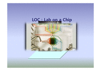
Why, Lab-On-a-Chip ?
Several Lab functions on a single chip
very Small size
Cheap – Mass
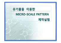
1. PURPOSE
MICRO-CHANNEL 제작 실험을 실행함으로써
반도체, 디스플레이 및 MEMS (Micro Electronic
Mechanical System) Micro Scale Patterning
공정 기술의 (Photo Lithography, Spin Coating,
Plasma Treatment 등) 원리를 이해한다.
2. THEORY
1) MEMS (Micro Electronic Mechanical System)
정의
- 기계와 전기 등 다방면의 기술이 관
recognition in nanoscale systems.
While microfabrication techniques such as photolithography, microcontact
printing, micromachining, and microwriting can produce patterns as small
as 0.1 mm, production of sub-100-nm structures still poses a significant
challenge.
At present, such high-resolution fabrication can be achieved using scanning
probe lithography (SPL).