Ⅰ. 서 론
1. 실험 목적
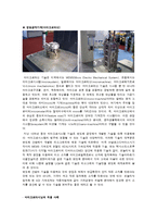
현재 magnetron sputter는 반도체, LCD 등을 포함하는 microelectronics 산업에서 박막 형성을 위한 주요 장비로 널리 쓰이고 있으며, 소자의 고집적화 및 대형화 추세에 따라 그 이용가치는 더욱 증대되고 있다. 본 연구에서는 TFT-LCD용 color filter제조시 ITO 박막 형성을 위해 사용하는 m
2.1.4. 스마트 그리드의 장·단점
장점 - 효율적인 전기 사용으로 전기료 부담 낮아짐
- 신·재생 에너지 확산으로 환경 보호 효과
- 안정적인 전기 공급
단점 - 네트워크 상 보안 문제 발생
2.2. 신재생에너지
2.2.1. 신재생에너지란?
기존의 화석연료를 변환시켜 이용하거나, 햇빛, 물, 지열,
RF MEMS, 그리고 의료 및 생체 응용을 위한 Bio-MEMS에 대한 연구개발이 선진국을 중심으로 활발하게 이루어지고 있다. 그리고 디스플레이에 응용하기 위한 마이크로미러 어레이(Micromirror array), 정보통신 및 자동화기기에 응용하기 위한 마이크로스위치, 의료용기기에 응용하기 위한 마이크로밸브 등은 제
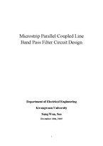
A filter is widely used in overall RF system. There are many species and structures in filter. A filter seems to be simple, but there are many considerations to design filter. In this paper, we design microstrip bandpass filter which has bandwidth of 500 MHz and center frequency of 2.5 GHz. Alumina is used as substrate, and chromium is used as conductor. Final results are achieved as follows. Ins
lambda: (1)source of revenues (2)manufacturing facilities (3)use of risk management products. We choose to use the first one; source of revenue.
Samsung SDI is a Korea company but we use risk free rate and risk premium as US T-bond, so we must adjust cost of equity by using country risk premium.
⑤ Three ways about estimating Ke
(1)Ke = Rf + β*MRP + CRP
(2)Ke = Rf + β*(MRP + CRP)
2. Experimental
2.1. Film preparation
Pure ZnO thin films were prepared on the glass substrate using RF magnetron sputtering system. And Mg, Ga doped (3 wt%) ZnO thin films were prepared on the ZnO pre-sputtered glass substrate using RF magnetron sputtering system. The PureZnO target was made from high purity ZnO powder (99.99 %) . The MZO/GZO targets were made from high purity ZnO powder (
High optical transmittance
Wide optical band gap
High electrical conductivity
Low cost
Non-toxicity
Good stability
Requirement of low temperature
Why is Wide band gap energy good?
It can be a very effective optoelectronic devices
There are many III-V and II-VI compound semiconductors with high bandgaps. The only high bandgap materials in…
group IV are diamond
Ge is an indirect band gap semiconductor with smaller energy difference between indirect gap and direct gap, and smaller effective masses for electron and hole pairs.
Small ionic radius difference between Ge ion and Zn ion.
These characteristics lead to the expectation that it is much easier to change the electronic structure around the band edge.
- The effects of doping and substrat
3.Result and Discussion
Fig. 1 shows the XRD patterns from the as-grown films. There is no new peak appearing when RF power of Ge is 0 W except for three peaks of ZnO (1 0 0), (0 0 2)and (0 0 4) located at 2θ = 30.888, 34.218, and 72.138, respectively. At RF power 100 W, these three peaks shift toward larger angle apparently and their intensity has also enhanced slightly. This indicates tha
A partially ionized gas created by application of an electric field. Positive ion/electron pairs are created by ionization reactions, maintaining overall charge neutral.
Commonly, radio-frequency (RF) at 13.56 MHz is used to create the glow discharge.
Typical pressures are between 1 mtorr and 5 torr.
Effective method for modifying surface property of a material little effect on bulk pro