Free(wannier-mott)
Radius >> a(exciton Bohr radius)
Small binding energy :~ 0.01 eV
Delocalized states
Move freely through crystal
(semiconductors)
Tighthly-bound(Frenkel)
Radius ~ a(exciton Bohr radius)
large binding energy : 0.1 -1.0 eV
localized on one lattice site
Moving by hopping
(insulators and molecules)
Eadd = △E + Ec
Ec = e2/C
C = 2πεεod
(depend on geometr
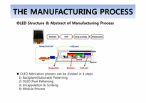
Glass/ITO/Cr substrate will be patterned by photolithography.
In AMOLED fabrication, TFT array is on the substrate. Anode electrodes is formed on that TFT. And these are covered with insulator.
PMOLED is formed anode, insulator, cathode separator in order.
This process form electrodes. Organic layer will be deposited on anode.
FMM method is used for small molecules materials
In high-degr
insulator.
Contains larger blood vessels and nerves than those found in the dermis
Burn
2nd degree
Damage in epidermis and partial dermis
Full thickness defect in dermis
Need skin graft
3rd degree
Damage in epidermis, dermis, hypodermis
Need skin graft
Ulcer
breakdown of the skin caused by fluid build-up in the skin from poor vein function (venous insufficiency).
Fluid leaks from t
성장시킨 실리콘 결정에는 전기전도도를 위해 의도적으로 첨가한 불순물(B,P,Sb) 이외에는 가능한 한 불순물을 억제시켜야 하며, 결정성장(Crystal Growing)시 인위적으로 주입되는 도판트(Dopant)에 의해 도체(Conductor)와 부도체(Insulator) 사이의 전기전도도를 가지며, 이를 반도체(Semiconductor)라고 한다.
Oxide formation temperature zones(1) 250-600℃ : Anodic oxidation, CVD, Sputerring(2) 600-900℃ : CVD (TEOS organic pyrolysis)(3) 900-1200 ℃ : Heat Oxidation(dry / wet)
dry oxidation
Usually due to excellent SiO2 surface properties used to form a thin oxide in the device structure
Si + O2 → SiO2
wet oxidation
Due to rapid growth rates used to form a thick
Layer. About 1
which correspond to the following conditions
1. The angle of incidence = angle of scattering.
2. The pathlength difference is equal to an integer number of wavelengths.
- Aluminum oxide
Electrical insulator
relatively high thermal conductivity
Trigonal, hR30
- Applications
Refractories, ceramics, polishing
Health and medical applications
Hard protective coating.
insulator with
a higher dielectric constant than silicon dioxide.
In such a scenario, a thicker gate layer might be used which can reduce the leakage current flowing through the structure as well as improving the gate dielectric reliability.
The drive current ID for a MOSFET can be written
(using the gradual channel approximation) as
Where
W : width of the transistor
Stable at high temperatures
in inert atmospheres
Surface oxidation occurs
Wurtzite structure
- Applications
LED
Military applications
Surface acoustic wave sensors
Properties AlN
Molar Mass 40.9882g/mol
Appearance White to pale-yellow solid
Band gap 6.2 eV
Density 3.260g/cm3
Melting Point 2200°C
Boiling Point 2517°C
Solubility in water Decomposes
Thermal Conductivi
II. Recent Situation of The Korean Economy
The Korea international trade had suffered much more than the Korean Financial Crisis with the IMF(1997 and 1998) than they had this year. With the constantly fluctuating prices and values for raw materials, exchange rates and the global financial crisis, it was an extremely difficult situation. A sudden rise in exchange rates cause losses in exchange
Insulation for Apparel (Thinsulate™)
Library Systems
Occupational Health & Environmental Safety
Personal Safety
Reflective Material (Scotchlite™)
Track & Trace Solutions
Traffic Safety Systems
Window Safety
Transportation Industry
Aerospace
Automotive
Marine
Specialty Vehicle
Traffic Safety Systems
Manufacturing & Industry
Abrasives & Sandpaper