thin,
curved, gleaming sharp.
-- MORE ANGLES, EVEN CLOSER. We can HEAR the MANs
wheezing BREATHING, but we still havent seen
his face. We never will. We just SEE more metal
being assembled with crude tools, into some sort
of linkage -- a splayed, spidery sort of apparatus,
against a background light of FIRE, and a deep
rushing of STEAM and HEAVY, DARK ENERGY.
-- And then we see this linkage attac
thin films formed by stepwise self-assemblyof ~6 nm Au particles and organic di- thiol on mercaptosilane-functionalized glass substrates. The thin films produced have been studied by UV/Vis spectroscopy, ellipsometry, scanning tunneling microscopy, and temperature-dependent conductivity measurements. The results show that the Au parti- cles are well-protected by the dithiol linker molecules and d
TFT LCD
THIN FILM TRANSISTOR LIQUID CRYSTAL DISPLAY
INTRODUCTION TO MICROELECTRONIC FABRICATION. PROFESSOR J.G PARK. EMPL
MATERIAL SCIENCE & ENGINEERING.
Hanyang University
INDEX
INTRODUCTION OF TFT-LCD.
THEORETICAL PRINCIPLE.
FABRICATION PROCESS.
OUTLOOK.
Hanyang University
INTRODUCTION
OF TFT-LCD
TFT-LCD
Hanyang University
TFT-LCD 란?
기존의 LCD는 PM(PASSIVE MATRIX)방식을 이용하여
1. 수치 해석
◉ Note
이번 실험에서 Fin은 2차원 형상인 Thin Rectangular Fin이다. 하지만 두께가 넓이에 비하여 매우 얇고 기부의 열원이 평행하게 작용한다고 가정하면 온도의 분포는 1차원으로 생각할 수 있다. 이 때 2차원 Fin을 1차원으로 가정할 수 있는 근거를 FDM을 이용하여 2차원 수치해석으로
Theory:
※IR spectrum
아래 Fig. 1의 IR spectrum은 일반적으로 흔히 사용되고 있는 IR spectrophotometer로 얻은 thin polystyrene film의 IR spectrum이다. 여기에서 알 수 있는 바와 같이, 가로축은 파수로 되어 있으며(파수로 할 경우 선형적이다) 세로축은 투광도(%)이다. 근래에는 사용 목적에 따라 두 축을 T-λ, A-λ 또는 A-
BulkGibbs free energy of formation of the amorphous oxide islarger than that of the corresponding crystalline oxide.
Thin filmThe thin amorphous metal-oxide film on its metal substrate can be stable modification with respect to the corresponding crystalline metal-oxide film the same substrate.
1. Interaction contribution to the - interfacial energy
Following the treat
Organic Light Emitting Diode(OLED)
An OLED is an electronic device made by placing a series of organic thin films between two conductors. When electrical current is applied, a bright light is emitted
A device that is 100 to 500 nanometers thick or about 200 times smaller than a human hair
Cheaper price
Less limited viewing angle
Higher contrast ratio
Easier to make
Less
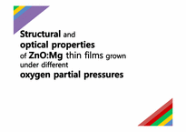
Pure and Mg-doped zinc oxide (ZnO:Mg)
films were deposited using RF reactive
magnetron sputtering at different oxygen
partial pressures.
◈ XRD ◈ SEM ◈ EDS ◈ PL
◈ Band gap ◈ Transmission Spectra
In this paper, ZnO:Mg thin films were
prepared on Corning 7105 glass substrate by
RF reactive magnetron sputtering technique
at different ratios of O2:Ar. The effects of Mg
do