Making the Wafer
The process
-A seed crystal is suspended in a molten bath of silicon
-It is slowly pulled up and grows into an ingot of silicon
-The ingot is removed and ground down to diameter
-The end is cut off, then thin silicon wafers are sawn off (sliced) and polished
Epitaxy
The growth of an ultra-pure layer of crystalline silicon
Approx 3% of wafer thickness
Contaminant-free
침전시켜야함을 인지하고 참고논문을 이용하여 STM(Sedimentation Time Modeling)을 유도하였다. 이러한 결과들을 종합하여 CMP 폐수의 유입부터 Microfiltration, Electrocoagulation 및 Sedimentation, 마지막으로 최종 pure water까지 공정을 설계하고 실제 산업에 적용 가능하도록 전반적인 Flow Diagram을 이끌어 낼 수 있었다.
2016년 12월 12일 주식을 코스닥 시장에 상장하였으며 주요 주주로는 임동준(6.49%), 조병호(6.28%), 임진환(5.4%) 등이 있다.
# 사업의 내용
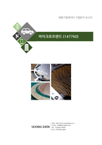
마이크로프랜드는 반도체 제조공정 중 반도체 소자의 전기적 기능의 검사를 위한 테스트 공정에 소요되는 프로브 카드(Probe Card)를 제조, 판매하고 있다.
반도체, 철강, 화학, 환경 산업분야에서 고순도 산소에 대한 수요는 급격하게 증가하고 있다.
공기로부터 산소를 생산하는 기술로는 전통적인 심냉법(Cryogenic process)이 일반적이다. 그러나 새로운 흡작제의 개발에 힘입어 200TPDs O2(ton per day contained) 생산 규모까지는 흡착공정이 생산 경쟁력을 확보하