


 분야
분야A-Si TFT 의 장점
1) 저온, 넓은 영역에 걸쳐 증착 가능
2) 다른 물질의 표면과 접착이 잘 됨
3) 내스크래치성, pattern화가 잘됨
4) 독성이 없음
5) 400도 이하에서 형성, 유리기판 사용 가능
inverted-staggered 구조를 만드는 공정방법은 크게 2가지가 있다.
etch stopper
Back Channel Etched 구조의 장단점
주요내용
[Cons]
[Pros]
successfully stick to surface of other material
3) 내스크래치성, pattern화가 잘됨
good scratch tolerance, patterning is easy
4) 독성이 없음
no toxic
5) 400도 이하에서 형성, 유리기판 사용 가능
glass substrate can be possible
inverted-staggered 구조를 만드는 공정방법은 크게 2가지가 있다.
for making inverted-staggered TFT we usually use these two method, BCE and ES
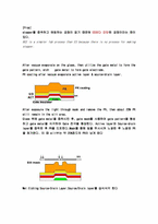
1.Etch stopper를 이용한 공정
2.Back-channel-etched(BCE)공정
-그림첨부-
etch stopper
1. 액정에 전압인가시 각 화소마다 독립적인 TFT소자를 통해 전압정보를 전달하는 방식으로 TFT의 구조에 따라 Bottom gate구조(Etch stopper stagger type, Back channel etched stagger type)와 Top gate구조(Coplanar type, Stagger type)로 구분된다.
-The structures of TFT that follow the method delivering the voltage information through the TFT elements of each pixel when appling the voltage are divided into Bottom gate structure including etch stopper stagger type , Back channel etched stagger type and Top gate structure including Coplanar type, Stagger type.
2. Amorphous Silicon은 보통 staggered TFT가 사용되는데 그 이유는 a-Si:H의 높은 resistance때문이다.
Resistance 때문에 Gate와 overlap되는 source와 drain이 있는 TFT는 좋은 전기적 특성을 가지게 된다.
-Amorphous silicon is usually used for staggered TFT, because of the high resistance of a-Si:H.
Due to the resistance, the TFT where source & drain overlap with gate shows good electrical characteristics.
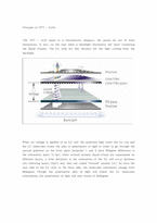
1. 증착 순서: 비정질 실리콘 위에 질화막을 연속으로 증착한 후 질화막을 패턴닝한다. 패턴닝된 질화막의 위에 n+층을 증착하고 그 위에 소오스-드레인 전극을 형성한다.


