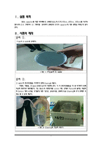
서 ③.
Si wafer에 Thermal&E-beam Evaporator를 이용해 SiO2를 증착시킨다. 이 때 E-beam을 이용하게 되고 PVD(Physical Vapor Deposition)증착법을 사용하기 때문에 내부는 진공상태를 유지한 채 증착을 시킨다. Thermal&E-beam Evaporator에는 E-beam과 Thermal 방법이 있는데 고융점 재료에 E-beam을 이용하게 된다.
★진공을 뽑아 주
Tungsten filament was
heated to generate electron.
Revolving 270, the electrons
are directed by
electromagnetic field
resulting collision onto the
source surface
After heated to certain
degree, source gas was
generated
The sensor monitors the
thickness of deposited film.
High vacuum should be kept in
the chamber not to contain
oxigen
gas which damages
substrat
Patterning : Photo Lithography
(Clear than Shadow Mask)
PHOTO LITHOGRAPHY
PROCEDURE:
1. Coat the PR
2. Expose to UV light
through the Mask
3. Immerse the plate
in the “Developer”
5. Coat metal
6. “Lift-off” in acetone
Pressure : 6.4 X 10⁻⁵ torr
Deposition : 1.2nm
Why we use E-beam Evaporator?
- Good growth rate and step coverage
3. a-IGZO기반
Oxide
TFT문제점
채널층에서 발생하는 문제
① 대기 중 산소나 수분과
금속의 자유전자가 반응
=> 자유전자 감소
② 빛에 의해 정공이 생성 됨
=> 정공 증가
↓
전기특성 신뢰도 감소
Transistor Switching 원리
채널이 형성되어
Source와 Drain간에
전류가 흐르기