듐 방사선에서 알파선과 베타선 이외에 투과성이 매우 강한 감마선이 있음을 알아내었습니다.
그림 11.1을 보시면 방사선이 전기적으로 대전된 판에 의해서 3가지요소로 나눠지는 것을 볼수있습니다. 첫성분은 음전하를 띠는 판으로 끌어 당겨졌고 그래서 양전하를 띤다. 이것을 알파입자입니다. 양전
The GZO, MZO thin films were prepared on ZnO pre-sputtered glass substrate using RF Sputtering Technique. Morphological, Structural and Electrical properties of deposited films were investigated in comparison with pure ZnO Thin film by scanning electronic microscopy (SEM), Atomic force microscopy (AFM), X-ray diffraction (XRD), PL spectra and other electrical analytic method. SEM images showed al
films was obtained using X-raydiffraction (XRD) spectra (X’ pert PRO, Phillips. Eindhoven, Netherlands). The surface morphology and roughness of the films was observed by field emission scanning electron microscopy (FE-SEM, Model: JSM-6701F) and atomic force microscopy (AFM, Digital Instrument, nanoscope III) operated at room temperature, respectively. The electrical properties of the films wer
WHAT IS THIN FILM?
KIST Definition (1991)
- Thin Film : 기판층(substrate layer)에 형성된 수 m 이하의 두께를
갖는 것으로 독립적인 기능을 보유한 막.
ADVANTAGES OF THIN FILM
Complexibility and Accumulations
Easy processing
lm)
Easy Control of Thermal, Mechanical and Chemical Properties
Down the Cost of Production
High-Reliance
WHAT IS cvd?
Principle of cvd
atoms fly to a target and stick onto the
surface
Source material is coated onto the target
surface
ADVANTAGE
Simple process
Fast deposition speed
Cheap process device
1. Partially different thickness
2. Difficult to control the element ratio
3. Hard to deposition the complex material layer
4. Low film quality
3.Material to be evaporated by e-beam
- E-beam dashes
ⅲ. Disarmament of Conventional Weapons
The first UN Conference on the Illicit Trade in Small Arms and Light Weapons in All its Aspects adopted in July 2001 a forward-looking program of action that committed nations, regions and the international Community collectively to:
1) Help to prevent, combat and eradicate the illicit trade in small arms
2) Enhance cooperation among states to end
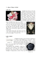
bomb)’ 속으로 들어가면 웅장하고 거대한 궁전에 도착하게 된다. 신비로운 선율이 흐르면서 성의 모습이 뚜렷하게 보이며, 마우스 커서를 움직이는 방향으로 성 내부를 둘러볼 수 있게 고안되어 있다. 각 방을 클릭하면 검은 리본과 함께 ‘빅터앤롤프’를 더 자세히 알아볼 수 있는 시간을 가질 수 있
3D printing
3D printing or additive manufacturing (AM) refers to any of the various processes for printing a three-dimensional object. Primarily additive processes are used, in which successive layers of material are laid down under computer control. These objects can be of almost any shape or geometry, and are produced from a 3D model or other electronic data source.
Basic principles
If the
The threshold voltage of a MOSFET is usually defined as the gate voltage where an inversion layer forms at the interface between the insulating layer (oxide) and the substrate (body) of the transistor. The purpose of the inversion layer's forming is to allow the flow of electrons through the gate-source junction. The voltage of oxide is given by
V_OX= 1/C_OX 2√(qN_A ε_Si V_0 )
SiO_2 V_O