films was obtained using X-raydiffraction (XRD) spectra (X’ pert PRO, Phillips. Eindhoven, Netherlands). The surface morphology and roughness of the films was observed by field emission scanning electron microscopy (FE-SEM, Model: JSM-6701F) and atomic force microscopy (AFM, Digital Instrument, nanoscope III) operated at room temperature, respectively. The electrical properties of the films wer
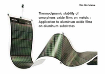
film on its metal substrate can be stable modification with respect to the corresponding crystalline metal-oxide film the same substrate.
1. Interaction contribution to the - interfacial energy
Following the treatment given in Sec. III A1 for the interaction energy across the crystalline-amorphous- interface
1. the difference in ⅰ)bulk ⅱ)surface ⅲ)interfacial
surface
ADVANTAGE
Simple process
Fast deposition speed
Cheap process device
1. Partially different thickness
2. Difficult to control the element ratio
3. Hard to deposition the complex material layer
4. Low film quality
3.Material to be evaporated by e-beam
- E-beam dashes against
material
- E-beam transport energy
to the material
- Then evaporation process
Film)과 하판(Film 또는 Glass)으로 구성되며, 터치된 지점의 상하판이 접촉되어 전기적인 Analog X, Y 신호를 검출하고, 그 신호를 Touch Controller로 전송하는 기능을 담당한다. Touch Controller의 경우 터치 패널에서 전송된 전기적인 Analog 신호가 Touch Controller의 A/D Converter에 의해 디지털 신호로 수치화하여 각 운영