Cu/In 비에 따른 CuInS2 박막의 특성에 관한 연구
A Study on Properties of Cu/In ratio on the CuInS2 thin film
Abstract
CuInS2 thin films were synthesized by sulpurization of Cu/In Stacked elemental layerdeposited onto glass Substrates by vacuum furance annealing at temperature 200[℃].
And structural and electrical properties were measured in order to certify optimum conditi
LayerDeposition
Dry oxidation이용하여 산화시킨다.
③ Heat Treatment
④ Au 증착
E-beam Evaporator를 이용하여 Si-SiO2 기판에 Au를 증착한다.
Mask의 직경은 각각 1mm, 2mm, 3mm이다.
⑤ 폴리싱 후 Ag Plate를 바른후 굳힌다.
⑥ C-V, I-V를 측정한다.
Au 증착
Au 증착 Mask
Ag Plate 바른 기판
Ag Plate 바른 시편
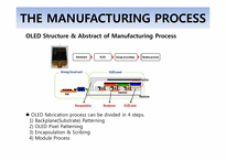
Glass/ITO/Cr substrate will be patterned by photolithography.
In AMOLED fabrication, TFT array is on the substrate. Anode electrodes is formed on that TFT. And these are covered with insulator.
PMOLED is formed anode, insulator, cathode separator in order.
This process form electrodes. Organic layer will be deposited on anode.
FMM method is used for small molecules materials
In high-degr
1. Cleaning
- For elimination particle
2. Deposition
- Formation some material layer on the substrate
3. Photolithography
- Formation some pattern
4. Etching
- Elimination substrate or PR layer
Material to be evaporated is heated to
increase vapor pressure
In a reasonably high vacuum, material
atoms fly to a target and stick onto the
surface
Source materi
of single srystalline solar cell
2. Structure
1) PESC [Passivated Emitter Solar Cell]
light absorption surface
– Inverted pyramids structure, double
reflection prevention layer
front – oxide passivation, electrode
passivation by narrow elctrode area
rear – Al deposition, form p+ layer
electrode
open circuit voltage - below 670 mV
OLED의 성장조건에 따른 X-선 산란 연구
Introduction
Tris-(8-hydroxyquinoliolato) aluminum(Alq3)
C27H18AlN3O3
Organic Light Emitting Diode
(Green light emitting, Electron Transport Layer)
Dependent on deposition condition
Change the temperature of the substrate
Previous study
deposition of ink droplets to form a line of drawing or of text. When the paper advances the width of the line, the next pass of the nozzle deposits a slightly different pattern. Thus line by line the complete text or the drawing is formed. After the whole page has been printed, a new sheet of paper is inserted and a new text or a new drawing is created.
In 3D printing, after the first layer has
ITO? What another materials can be used?
How about flexible transparent plastic?
Yes, it’s flexible display!!
EIL: Electron Injection Layer
ETL: Electron Transfer Layer
EML: Emission Material Layer
HTL: Hole Transfer Layer
HIL: Hole Injection Layer
Backplane
OLED
Encap. & Scribing
Module process
1. Low work-functon
2. Easy deposition
3. Low activity
layer-by-layer growth model. It is noticed that under the bottom of nanorods, ZnO layer with the 608 angle between the nearest neighbors is formed on the side-wall of central axial nanowires, as shown with white arrow in Fig. 1(e) and (f); Meanwhile, the large nanoclusters are found existing on the bottom of nanorods, as shown with black arrows in Fig. 1(f). These observations imply the following
layer (SiON) is deposited on-to the substrate to prevent direct contact with air. The SiON has high resistance for water penetration and good mechanical properties to be used as encapsulation. This material can also be used as anti-reflection layer. The required index of refraction for this layer to act as anti-reflector is 1.9 and SiON has refractive index ranging from 1.8 to 2.0. By applying th