AlN의 형성은 열역학적으로 자발적인 반응
In-situ Al/AlN 복합재
알루미늄의 높은 열 전도도를 유지
열 팽창계수의 감소
비강도 증가
복합재의 제조 원가 절감
최대 50 wt% AlN이 형성되었음 R.G. Reddy et al (2007)
수 마이크로미터 크기의 AlN 입자 형성
AlN이 용탕의 상층부에 집중적으
방법론적으로는 먼저 chamber내에 존재하던 전자들이 전기장에 의해 운동에너지를 얻어 + 전압이 걸린 쪽으로 이동을 하게 되면서 그 과정에서 주변에 있던 gas atom들과 충돌을 하게 되고, 충격을 받은 gas atom에서 다른 전자가 나오게 되면서 radical이나 양이온이 되는 것으로 간략하게 볼 수 있다. 이렇게
2.3 C-V graph
The measured MOS capacitance (called gate capacitance) varies with the applied gate voltage.
① Measurement of C-V characteristics
-Apply any DC bias, and superimpose a small (15 mV) ac signal
-Generally measured at 1 MHz (high frequency) or at variable frequencies between 1KHz to 1 MHz
-The dc bias VG is slowly varied to get quasi-continuous C-V characteristics
② C-V chara
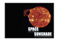
- How to send the lenses into orbit, in one piece. Since conventional rocket systems with fossil fuel are expensive and polluting, professor Angel hopes to use a coil gun. While it could take 30 years to perfect, this technology might possibly be a revolutionary breakthrough in space travel. Angel's plan is for 20 coil guns to be built around the world, buried deep in mountains. The vertical gun
Lenses are launched into the space
Lenses find their assigned position
Lenses play a role as blocker
Lens material properties required
-Regarding cost
-In order to keep costs down, the lenses will need to be as light as possible
-weigh around 0.04 ounces (1 gram)
-Regarding survivor
- 24/7 heat of the sunlight without changing its properties
ex)becomi
ML2 means the maskless lithography. It is necessary to refinement process. Described above, "double / mutiful patterning" in additional cost savings as an alternative to be appropriate. Nano devices with decreasing the size of the unilateral use light to produce a mask for the lithography process takes time and cost. Small production of nano scale patterning process is suitable, and the suitable
1. Purpose
Find the unknown specimens by using
XRD(X-ray diffractometer).
2. Theory
- Principle of XRD
A method for the structure
analysis
Using monochromatic X-ray
Involving interference of waves
described by Bragg’s law
- Bragg’s law
When x-rays are scattered from a crystal lattice, peaks of scattered intensity are observed which correspond to the fol
PE CVD
PE CVD공정은 Plasma etching 이 사용되기 이전부터 반도체 금속배선의 보호막인 SiN과 SiO2를 저온에서 증착할 수 있는 새로운 생성원으로 소개
PE CVD기술은 SiO2와 SiN 박막 형성 뿐만 아니라 최근에는 천이금속이나 천이금속 실리사이드 형성에도 널리 사용
PE CVD의 박막 형성 mechanism
Plasma 에서 이