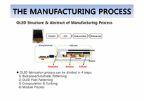
Glass/ITO/Cr substrate will be patterned by photolithography.
In AMOLED fabrication, TFT array is on the substrate. Anode electrodes is formed on that TFT. And these are covered with insulator.
PMOLED is formed anode, insulator, cathode separator in order.
This process form electrodes. Organic layer will be deposited on anode.
FMM method is used for small molecules materials
In high-degr
by PECVD
Isolation process
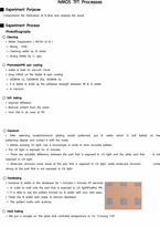
○ Photolithography
PR
SiO2
N-type
Si
N-type
⦁Deposit photoresist on SiO2.
SiO2
N-type
Si
N-type
⦁Expose UV light. The part of unexposed removes because of negative PR.
○ Wet etching
SiO2
N-type
Si
N-type
SiO2
⦁SiO2 that does not have PR is removed by
by showing the current condition of bus operations, and the distance between the earlier and following buses to manage the time in which buses arrive at the bus stops. It does so by collecting information through the BMS servers and wireless communication including the satellite on when the bus started its course, where it is located in its course, and the arrival and departure time and name of e
on present research findings, it can be seen that hydrogen production in cyanobacteria can be increased by blocking the function of uptake hydrogenase.
2) Limitation of Hydrogen Production
When the 9.5kb element is excised, the heterocyst form of the cell will produce uptake hydrogenase. Therefore we must inhibit the 9.5kb element that has the XisC unit or just the XisC enzyme.
3) Our
문제가 되는 반대쪽 전극의 손상이나 파티클 발생 등의 문제 해결 가능
1015 ions/cm2 이 300~ 700 eV 의 energy 로 표면과 충돌할 때 substrate 표면파괴 및 화학적인 오염이 심각함
residual film 형성
gas phase particle deposition
metallic impurities
불순물 제거 방법 : 습식 산화 제거에 의한 산소 또는 수소 plasma 처리
1.Photolithography
리소그래피는 포토레지스트를 도포하는 공정으로 시작해 노광, 현상, 에칭, 포토레지스트 제거에 이르는 일련의 프로세스이다. 현상까지를 레지스트 처리공정으로 하며, 에칭 공정과 분리해서 생각할 수도 있다. 현재, 패턴 노광은 레티클이라 불리는 마스크 기판에 의해 축소 투영 전
Pure and Mg-doped zinc oxide (ZnO:Mg)
films were deposited using RF reactive
magnetronsputtering at different oxygen
partial pressures.
◈ XRD ◈ SEM ◈ EDS ◈ PL
◈ Band gap ◈ Transmission Spectra
In this paper, ZnO:Mg thinfilms were
prepared on Corning 7105 glass substrate byRF reactive magnetronsputtering technique
at different ratios of O2:Ar. The effects of Mg
do
thinfilms produced byRFsputtering will have new advantage for industrial applications
It can be considered that physical properties such as optical, electrical and morphological of ZnO thinfilm produced byRFsputtering strongly depend on O2 concentration during production
Thus, it can be possible to be adjusted for various industrial applications like window materials, optoelectronic devic
sputtered respectively. The patterns exhibit four crystal phases, i.e., hexagonal ZnO (JCPDS 36-1451), hexagonal Zn (JCPDS 04-0831), cubic Au (JCPDS 04-0784), and orthorhombic Au2O3 (JCPDS 43-1039). The ZnO-associated peaks are attributed to the ZnO nanowires. In addition, we surmise that the excessive Zn in the vapor is adsorbed on the solid surface, resulting in Zn peaks [12]. The inset of Fig.