Si3N4 at low conformity.
⇒ High growth speed up to 500 nm/min is possible.
∙ Deposit at low temperature because of plasma.
∙ High vacuum and taking long time.
⇒ Increase the temperature up to 250℃ despite of low temperature.
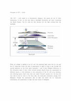
SiO2
N-typeSi
N-type
PECVD
Deposited SiO2 by PECVD
Isolation process
○ Photolithography
PRSiO2
type, Stagger type.
2. Amorphous Silicon은 보통 staggered TFT가 사용되는데 그 이유는 a-Si:H의 높은 resistance때문이다.
Resistance 때문에 Gate와 overlap되는 source와 drain이 있는 TFT는 좋은 전기적 특성을 가지게 된다.
-Amorphous silicon is usually used for staggered TFT, because ofthe high resistance of a-Si:H.
Due tothe resistance, the TFT where
is highly absorbed by all materials, even EUV optical components inside the lithography tool are susceptible to damage, mainly manifest as observable ablation. Such damage that is associated with the high-energy process of generating EUV radiation is a new concern specific to EUV lithography .
EUVL's shorter wavelength also increases flare, resulting in less than perfect image quality and incre
are shown in the bottom rows. The matched double patterning mask image placement must be tighter than a single mask overlay by the square root of 2. Therefore, the mask-to-mask overlay contribution in any particular location must be 20% ofthetotal pitch splitting error budget. The wafer CD error budgets for spacer patterning are also driven by the need to have both the line and space w
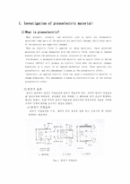
◎압전기 효과
압전기 효과에는 압전기 직접효과와 압전기 역효과가 있다. 전자의 압전기 직접효과란 압전소자에 외부응력, 진동변위 등을 가하면, 그 출력단에 전기 신호가 발생하는 현상을 말한다. 또한 후자의 압전기 역효과란 압전소자에 외부로부터 전압을 가하면 소자가 기계적 변위를 일