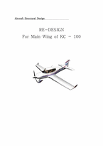
4. STRUCTURE DESIGN
4.1. Wing structure
Wing structure
The wing on the plane is a part that the highest load take. The large bending moments especially act on the point near the root of wing. Also, we should consider the number of spar, rib, position, skin thickness and taper ratio.
I Beam shape
4.2. I BeamBeam theory shows that the I-shaped section is a very efficient form f
1. 실험명 : Beam Test
2. Beam 실험관련이론
빔은 단지 모멘트가 적용되는 평면에서 가해지며, 빔의 응력 분포와 응력 곡률은
(1.1)
이 식에 의해 연관된다.
M : 굽힘 모멘트
I : 빔 절단공간의 2차 모멘트
E : 탄성계수
R : 곡률반경
f : 중립축으로부터 거리 y까지의 굽힘 응력
이것은 또한 빔의 굽힘이
[3] Thin Film Deposition
초집적 반도체를 구성하는 소자들은 그 특성상 그 크기가 매우 얇아(작고) 미세한 조직을 가진다. 그리고 이것은 박막 증착(TFD = Thin Film Deposition) 공정을 통해 제작된다. 박막 증착이란 이름 그대로 표면에 얇은 막을 씌우는 기술을 뜻하는데 이 공정을 통해 기판(substrate)이나 이전에
2.3 C-V graph
The measured MOS capacitance (called gate capacitance) varies with the applied gate voltage.
① Measurement of C-V characteristics
-Apply any DC bias, and superimpose a small (15 mV) ac signal
-Generally measured at 1 MHz (high frequency) or at variable frequencies between 1KHz to 1 MHz
-The dc bias VG is slowly varied to get quasi-continuous C-V characteristics
② C-V chara
Theories)
3.1. Si 특성
그림1. 초크랄스키법으로 제작된 단결정
실리콘은 금속과 비금속의 특징을 모두 가지는 전형적은 반도체소자로서 탄소족인 14번 원소이다. 자연에서는 단결정 형태로는 거의 존재하지 않으며 대부분 이산화규소나 규산염의 형태로 존재한다. 하지만 단결정 실리콘의 경우