Metal layer을 형성, 이후 진행될 공정의 기반이 될 substrate층을 완성하려 한다.
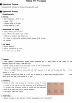
Process Sketch Related Materials Related Hardware
(Chamber/Equipment) Note
Step1
Form Al2O3 Ingot
With CZ process ㅡ Al2O3 Czochralski Furnace Al2O3의 Polycrystal 을 사용한다.
Step2
Cutting & Grinding ㅡ Al2O3 powder / Glycerin Diamond grinder
Step3
Chemical etching HF-HNO3-
Making the Wafer
The process
-A seed crystal is suspended in a molten bath of silicon
-It is slowly pulled up and grows into an ingot of silicon
-The ingot is removed and ground down to diameter
-The end is cut off, then thin silicon wafers are sawn off (sliced) and polished
Epitaxy
The growth of an ultra-pure layer of crystalline silicon
Approx 3% of wafer thickness
Contaminant-free
process of deposition of oxide layer. When the charges exist in between the substrate and interface, the value of Vfb and C-V curve will shift by amount of the charge divided by Cox of Ci. The amount of shifting decreases as the position of fiexed charges is far from interface on the substrate and shifting will not exist any more when it is located on the interface between metal and interface. Mo
○ PECVD
∙ What is PECVD?
⇒ Radio frequency(RF) is used to induce plasma in the deposition gas.
⇒ This results in a higher deposition rate at relatively low temperatures.
⇒ With the plasma enhanced CVD process is the deposition at temperature around 300℃ allows.
⇒ The temperature will be through encouragement of a plasma with high frequency electric fields triggered.
metals, especially at high temperature and pressure. The catalyst in commercial ammonia synthesis is usually an iron oxide mixed with a small amount of additional "promoter" material. When the process begins, the hydrogen gas converts the catalyst to pure iron. Gradually, as the iron catalyst is poisoned by carbon and sulfur compounds, it becomes less effective and must be replaced. Nitrogen gas