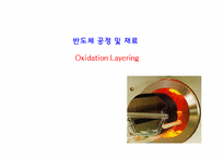
4. Dopant Barrier <불순물 장벽>
- 산화층이 실리콘 표면에서 성장하면 불순물 물질이 wafer로 들어가는 곳에 창을 생성시키기
위해서 Mask 개방으로 SiO2를 식각, 이때 산화물은 dopant의 확산으로부터
silicon의 표면을 보호.
- 선택적인 dopant의 도핑가능
5. 금속층 사이의 유전체
silicondioxide)
ε0 is the permittivity of free space
decreasing the thickness t -> increase the capacitance of the structure
increase the number of charges in the channel and the drive current for a
fixed value of gate voltage.
the silicondioxide layer thickness is reaching the limits of scaling.
The alternative way of increasing capacitance is to use an insulator with
Crosstalk among neighboring interconnects
Capacitive crosstalk roughly proportional to kc=CIMD /CILD
⇒ Mainly fixed by the aspect ratio of lines and vias
⇒ Crosstalk level increases at each new generation
Induces delay uncertainty
A low-κ dielectric materials with a dielectric constant less than the dielectric constant of silicondioxide, κ<4
First low-κ was applied at the
silicondioxide or gallium arsenide wafer등의 기판에서 감광층을 선택적으로 노출시키기 위해 사용된다.
Wafer는 positive photoresist으로 개발되고, 노출된 부분은 화학적 과정으로 제거된다.
wafer 표면에 남겨진 모양은 노출에 의해 덮혀져 있던 부분이다.
TEM exposure
웨이퍼의 through hole은 TEM(투과전자현미