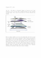
Etch stopper를 이용한 공정
2.Back-channel-etched(BCE)공정
-그림첨부-
etch stopper
1. 액정에 전압인가시 각 화소마다 독립적인 TFT소자를 통해 전압정보를 전달하는 방식으로 TFT의 구조에 따라 Bottom gate구조(Etch stopper stagger type, Back channel etched stagger type)와 Top gate구조(Coplanar type, Stagger type)로 구분된다.
-The
Etching system
주로 화학적인 반응에 의해 에칭 진행
이온의 충돌에 의한 이방성 에칭이 되기 어려움
아래 위 두 전극의 크기는 거의 같이 보이지만
반응관 벽면은 접지되어 있으므로
RF가 인가되는 전극에 비해 웨이퍼가 올려져 있는 접지된 전극의 면적이 훨씬 크다.
Reactive Ion Etching system
충돌하
1. Dry Etch; PR 등의 보호막으로 가려져 있지 않은 부위의 막질 제거
2. Ashing; PR 제거
3. Plasma Nitridation; 얇은 산화막 등 유전막의 특성 개선을 위한 표면 처리
4. Plasma Oxidation; Transistor의 특성 개선을 위한 표면 처리
5. 유전막 PE-CVD (Plasma Enhanced Chemical Vapor Deposition); SiON 등의
유전막 증착
6. Barrier Meta
side Metal layer을 형성, 이후 진행될 공정의 기반이 될 substrate층을 완성하려 한다.
Process Sketch Related Materials Related Hardware
(Chamber/Equipment) Note
Step1
Form Al2O3 Ingot
With CZ process ㅡ Al2O3 Czochralski Furnace Al2O3의 Polycrystal 을 사용한다.
Step2
Cutting & Grinding ㅡ Al2O3 powder / Glycerin Diamond grinder
Step3
Chemical etching HF-
Its magnified and deeply revealed. Flecks of green and yellow in a field of milky blue. Icy filaments surround the undulating center.
The eye is brown in a tiny screen. On the metallic surface below, the words VOIGHT-KAMPFF are finely etched. Theres a touch-light panel across the top and on the side of the screen, a dial that registers fluctuations of the iris.
The instrument is no bigger than a