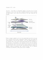
TFT가 사용되는데 그 이유는 a-Si:H의 높은 resistance때문이다.
Resistance 때문에 Gate와 overlap되는 source와 drain이 있는 TFT는 좋은 전기적 특성을 가지게 된다.
-Amorphous silicon is usually used for staggered TFT, because ofthe high resistance of a-Si:H.
Due tothe resistance, theTFT where source & drain overlap with gate shows good electrical character
we use Sputter?
- Good for high Melting point Material
- Thickness uniformity
- Positive adhesion
- But, law growth rate and step coverage
Patterning : Photo Lithography
(Clear than Shadow Mask)
Why Al is used for electrode?
(Especially Gate)
- Law melting point
- Work function
- High-K, Good mobility
- Elimination of carrier mobility degradation
→ ALD is based on the sequential use of a gas phase
chemical process. ALD film growth is self-limited and
based on surface reactions, which makes achieving
atomic scale deposition control possible.
☞ Self-limited growth
☞ Atomic scale deposition
☞ Easy way to produce
uniform, crystalline,
high quality thin films.
-결정성 평가
-FWHM (Full wi
CRT(Cathode Ray Tube)
A vacuum tube in which a hot cathode emits electrons that are accelerated as a beam through a relatively high voltage anode.
Composed of fluorescent tube, shadow mask., electron beam
flexible substrate technology
-flexible glass
-flexible steel(metal foil)
-plastic film
-complex material sheet
ofthe material (3.9 for silicon dioxide)
ε0 isthe permittivity of free space
decreasing the thickness t -> increase the capacitance ofthe structure
increase the number of charges in the channel andthe drive current for a
fixed value ofgate voltage.
the silicon dioxide layer thickness is reaching the limits of scaling.
The alternative way of increasing capacitance isto