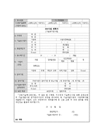
공정과정의 종류를 변수로 놓고, 각 device별로 C-V와 I-V를 측정하여 각각의 변수가 Capacitance와 Current에 어떤 영향을 미치는지에 대하여 분석해 본다.
2. 실험이론
① MOSCapacitor
(a) MOSCapacitor의 구조
MOScapacitor의 구조
MOS는 Metal-Oxide-Semiconductor의 약자로, 금속 층과 반도체 물질로 되어 있는 두 개의
MOS-capacitor on p- and n-type Si
The C-V data depends on the measurement frequency as well.
[Figure 11] Measured C-V characteristics on an P-type, N-type Si
2.4 Graph shifting
In MOS structure, we should consider non ideal effects when measure the capacitance according to applied voltage. They are 'fixed charge', 'mobile charge', and 'surface states'. When the fixed charge exists in
4. Equipment
4.1 RCA cleaning
RCA cleaning is a series of rinsing procedure prior to experiment with Si wafer. The purpose of the RCA clean is to remove organic contaminants (such as dust particles, grease or silica gel) from the wafer surface. There are three steps to be performed. The first step is to remove organic contaminant from surface of wafer. Second step is to remove any oxide layer
실험적인 데이터를 통해 계산한 후 실제 값과 비교하여 본다.
1-2 배경 이론
1-2-1 MOSCapacitor
그림 1.1 Capacitor
그림 1.2 MOScapacitorCapacitor(축전기)란 전기회로에서 전기용량을 지녀 전하를 축적시키는 소자를 지칭한다. MOSCapacitor란 Metal-Oxide-Semiconductor(금속-산화물-반도체)의 3중 구조를 말한
MOSCapacitor의 C-V 및 I-V 그래프의 변화를 보기위하여 변수를 3가지 SiO₂ 두께(100nm, 200nm, 300nm)로 설정하였고, 통제 변인으로는 metal을 Ti로 정하였다.
3. 이론배경 (Theories)
3.1. Si 특성
그림1. 초크랄스키법으로 제작된 단결정
실리콘은 금속과 비금속의 특징을 모두 가지는 전형적은 반도체소자