2.양성 PR과 음성 PR의 화학식, 구조식 작동원리에 대해 설명하라
1.Photolithography란?
Photolithography 공정은 어떤 특정한 화학약품(Photo resist)이 빛을 받으면 화학반응을 일으켜서 성질이 변화하는 원리를 이용하여, 얻고자 하는 pattern의 mask를 사용하여 빛을 선택적으로 PR에 조사함으로써 mask의 patter
○ PECVD
∙ What is PECVD?
⇒ Radio frequency(RF) is used to induce plasma in the deposition gas.
⇒ This results in a higher deposition rate at relatively low temperatures.
⇒ With the plasma enhanced CVD process is the deposition at temperature around 300℃ allows.
⇒ The temperature will be through encouragement of a plasma with high frequency electric fields triggered.
Lithography
Types of Photolithography Processes
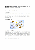
Photoresists 는 빛, 전자에 민감한 감광성의 중합체로서 positive 와 negative의 두 가지 타입으로 나눌 수 있다.
Positive: 마스크와 같은 형상을 새김
Negative: 마스크와 반대 형상을 새김
Stereo lithography (3차원 리소그라피)
가장 널리 쓰이는 형상 구현 기술
액
※반도체 제조공정 중 기존의 lithograph 공정과 잉크젯 프린팅 공정의 차이와 잉크젯 프린팅 공정을 적용하였을 경우 얻어지는 장점
A. 반도체 제조공정 중 기존의 lithograph 공정
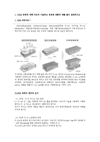
1.Photolithography
리소그래피는 포토레지스트를 도포하는 공정으로 시작해 노광, 현상, 에칭, 포토레지스트 제거에 이르는
위의 두 식을 살펴보면 Gate voltage가 상승하게 되면 처음 slope가 상승하게 되고 따라서 saturation voltage도 상승하게 된다. 또한 여기서 Cox는 εox/xox이므로 oxide층의 두께가 두꺼워질수록 앞서본 Vth에 대한 식에 따라 Vth가 커져 ID-VG그래프가 우측으로 shift하게 되고, 그래프의 slope역시 Cox가 작아짐에 따라 줄
[3] Thin Film Deposition
초집적 반도체를 구성하는 소자들은 그 특성상 그 크기가 매우 얇아(작고) 미세한 조직을 가진다. 그리고 이것은 박막 증착(TFD = Thin Film Deposition) 공정을 통해 제작된다. 박막 증착이란 이름 그대로 표면에 얇은 막을 씌우는 기술을 뜻하는데 이 공정을 통해 기판(substrate)이나 이전에
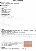
Lithography
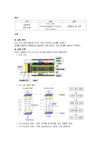
Si Wafer coated with PR
Spin coating
PR is coated evenly by turning round rapidly.
Exposure
Align the Mask exactly and emit UV.(fixed 10sec)
Observation
See the completed sample through SEM
Development
∙ Dip the sample in the alkaline solution.
→(process parameter : 10sec 60sec 180sec)
∙ Due to differences in solubility of the exposed portion to be dissolv
서론
▶ 실험 목적
Auto CAD 프로그램으로 자신이 직접 디자인한 Mask를 그려본다.
장비를 이용하여 포통공정과 셀공정에 대해 배우고, 직접 장비를 사용하여 익혀본다.
▶ 실험 이론
우리가 실험에서 쓰인 TN N/W mode에 대해서 간단히 설명하였다.
▸ Cell 구조
▸ TN LCD 동작 원리
▸
Making the Wafer
The process
-A seed crystal is suspended in a molten bath of silicon
-It is slowly pulled up and grows into an ingot of silicon
-The ingot is removed and ground down to diameter
-The end is cut off, then thin silicon wafers are sawn off (sliced) and polished
Epitaxy
The growth of an ultra-pure layer of crystalline silicon
Approx 3% of wafer thickness
Contaminant-free